AI Growth Meets Sustainable Semiconductor Manufacturing
AI is increasing semiconductor fab complexity. Learn why point-of-use waste gas treatment is becoming critical infrastructure for sustainable future fabs.

Executive Summary
AI is accelerating semiconductor growth and driving new manufacturing investment in the United States, increasing demand for advanced process technologies and additional wafer capacity.
Advanced chip manufacturing requires increasingly complex production environments, including sophisticated process steps and specialized gases and chemicals.
Point-of-use abatement technologies treat complex waste gas streams directly at the source, making effective waste gas treatment an important part of advanced fab infrastructure.
Energy, resource efficiency, and environmental systems are becoming increasingly important in U.S. fab planning and operation as semiconductor and digital infrastructure expand.
Future fabs will need to combine performance, efficiency and sustainability, making environmental technologies an integral part of advanced semiconductor manufacturing.
AI Growth Is Changing More Than Chips
Artificial intelligence has become a major growth driver for the semiconductor industry. Training and deploying large AI models requires enormous computing power, increasing demand for GPUs, AI accelerators, advanced logic and high-performance memory.
For semiconductor manufacturing, this means more than increasing chip output. Additional wafer capacity is needed, advanced process technologies are expanding, and manufacturers are investing in new production facilities. This development is particularly visible in the United States, where major semiconductor manufacturers are building and expanding domestic manufacturing capacity.
But scaling semiconductor production is not simply about building more fabs. AI-driven demand is contributing to the need for more complex manufacturing ecosystems.
Advanced devices require sophisticated process technologies, specialized gases and chemicals, extensive utility infrastructure and environmental systems capable of supporting increasingly demanding production requirements.
The result is a chain reaction: Growing demand for AI drives the need for more powerful chips, which require increasingly complex manufacturing processes and place new demands on semiconductor fabs.
Power, water, process gases, waste gas and wastewater treatment, and other utilities are therefore becoming increasingly important in the planning and operation of advanced semiconductor fabs in the United States.
More advanced chips mean more complex manufacturing
Semiconductor manufacturing already involves several hundred highly controlled process steps. As device architectures and manufacturing technologies become more sophisticated, the demands placed on production equipment and supporting infrastructure continue to evolve.
Advanced semiconductor manufacturing involves complex sequences of processes such as lithography, etching and deposition. These processes, along with associated chamber cleaning cycles, require a range of specialized gases and chemicals. Each process has its own requirements for supply, exhaust and environmental treatment systems.
Many critical process steps, including etching and chemical vapor deposition (CVD), rely on specialized fluorine-containing gases for wafer processing and chamber cleaning. The U.S. Environmental Protection Agency (EPA) specifically identifies semiconductor manufacturing processes using reactive fluorine-containing compounds for etching and chamber cleaning as sources covered under electronics manufacturing greenhouse gas reporting requirements.
For fab operators, this brings another question into focus beyond process performance: How can the resulting waste gas streams be treated reliably and efficiently?
Learn more about environmental solutions for the Semiconductor Industry.
“The sustainability performance of an abatement system should be measured by its overall climate impact. For gases such as CF₄, every fraction of a percentage point in DRE matters. By achieving destruction efficiencies above 99.9%, modern burn-wet technologies can significantly reduce residual greenhouse gas emissions and, despite the use of natural gas, contribute positively to a fab’s overall decarbonization strategy.”

Semiconductor fab emissions: Why fluorinated gases matter
Fluorinated greenhouse gases such as CF₄, NF₃ and other fluorinated compounds are particularly relevant from a climate perspective. Their properties make them valuable for semiconductor manufacturing processes, but they can also present significant environmental challenges.
CF₄ is a prominent example. It is used in semiconductor manufacturing, particularly in plasma-based processes. At the same time, its high chemical stability contributes to its long atmospheric lifetime and makes effective decomposition technically demanding.
As advanced semiconductor manufacturing expands in the United States, managing these process emissions becomes part of a broader engineering challenge. Fabs need to increase manufacturing capacity while simultaneously addressing environmental impact, energy efficiency and resource consumption.
As production volumes increase, the focus shifts beyond the number of chips being produced to how the associated emissions can be effectively controlled.
Deep Dive: Why does >99.9% DRE matter for CF₄ abatement?
Explore how high destruction and removal efficiency can influence semiconductor emissions. Beyond Industry Benchmarks: Why >99.9% DRE Matters
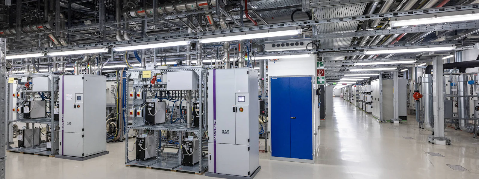
Point-of-Use Abatement: Treating waste gases at the source
One important approach is point-of-use waste gas abatement. Instead of relying solely on centralized treatment farther downstream, point-of-use systems treat waste gases close to the semiconductor process tool where they originate.
Depending on the process and waste gas composition, different abatement technologies can be applied to destroy or remove hazardous and climate-relevant compounds before the treated gas stream enters the downstream exhaust infrastructure.
Chemical vapor deposition (CVD) provides one example of where process-specific waste gas treatment plays an important role. CVD tools can generate waste gas streams containing fluorinated compounds, particularly during chamber cleaning. Gases such as NF₃ may be used to generate reactive fluorine species for this purpose. Point-of-use abatement systems treat these gases directly at the process tool and can be tailored to the specific requirements of each application.
Explore waste gas treatment for CVD processes: UPTIMUM
Explore Point-of-Use Waste Gas Treatment
Different semiconductor processes create different waste gas challenges. Discover how DAS Environmental Experts combines multiple treatment technologies to address complex process gases directly at the point of use.
Explore our waste gas treatment technologies:
From support equipment to fab infrastructure
Traditionally, environmental technologies have been viewed primarily as supporting systems required to meet emissions regulations. As semiconductor manufacturing becomes more complex and scales to higher production volumes, this role is changing.
Waste gas treatment is no longer defined solely by treatment capacity and destruction efficiency. System availability, redundancy, resource consumption and integration into the subfab all influence how reliably and efficiently new process requirements can be supported.
As a result, environmental technologies are increasingly becoming a strategic part of fab infrastructure. They must scale alongside production requirements without automatically increasing resource consumption and environmental impact at the same rate.
A well-integrated abatement strategy can support
effective treatment of complex semiconductor waste gas streams,
reduction of direct process emissions,
stable and reliable fab operations,
reduced load on downstream exhaust infrastructure,
efficient use of utilities and resources, and
scalable infrastructure for new process requirements.
The implication is clear: environmental technology should be considered as part of fab and process planning rather than added as an afterthought.
The next challenge: Scaling output without scaling environmental impact
The expansion of semiconductor manufacturing in the United States is taking place at the same time as AI is increasing electricity demand across digital infrastructure. Large data centers require substantial amounts of power, while semiconductor fabs themselves are highly energy-intensive manufacturing facilities that depend on stable and reliable utility infrastructure.
This creates an additional challenge for U.S. semiconductor growth. Expanding manufacturing capacity requires not only process equipment and production space, but also the energy, water and environmental infrastructure needed to operate increasingly complex fabs.
For fab operators, efficiency therefore needs to extend across the entire manufacturing environment, from process tools and facility infrastructure to environmental systems and water and wastewater management. As fabs become larger and more complex, energy and resource strategies are becoming important considerations in site planning, fab design and long-term operations.
Less Is More: Efficient Use of Resources in the Semiconductor Industry
Advanced waste gas abatement is one part of this picture. Water recycling and reuse, energy recovery, intelligent system control and resource-efficient operation are others. The objective is not merely higher output — it is higher output with a lower environmental impact per unit of production.
This changes the definition of fab performance. Production capacity and process stability remain essential, but they increasingly need to be considered alongside energy efficiency, resource management and environmental performance.
Summary: Turning the AI challenge into an engineering opportunity
AI is accelerating the evolution of the semiconductor industry. At the same time, increasingly advanced manufacturing processes are raising the requirements for the systems that enable production and help limit its environmental impact.
Point-of-use waste gas treatment and other environmental technologies are becoming essential building blocks of fab infrastructure that combines performance, scalability and sustainability.
The challenge is no longer only to produce more powerful chips, but also to build the infrastructure required to manufacture them responsibly with a lower environmental impact.